- 您现在的位置:买卖IC网 > Sheet目录3890 > PIC16C765T-I/L (Microchip Technology)IC MCU OTP 8KX14 USB 44PLCC
PIC16C745/765
DS41124C-page 38
Preliminary
2000 Microchip Technology Inc.
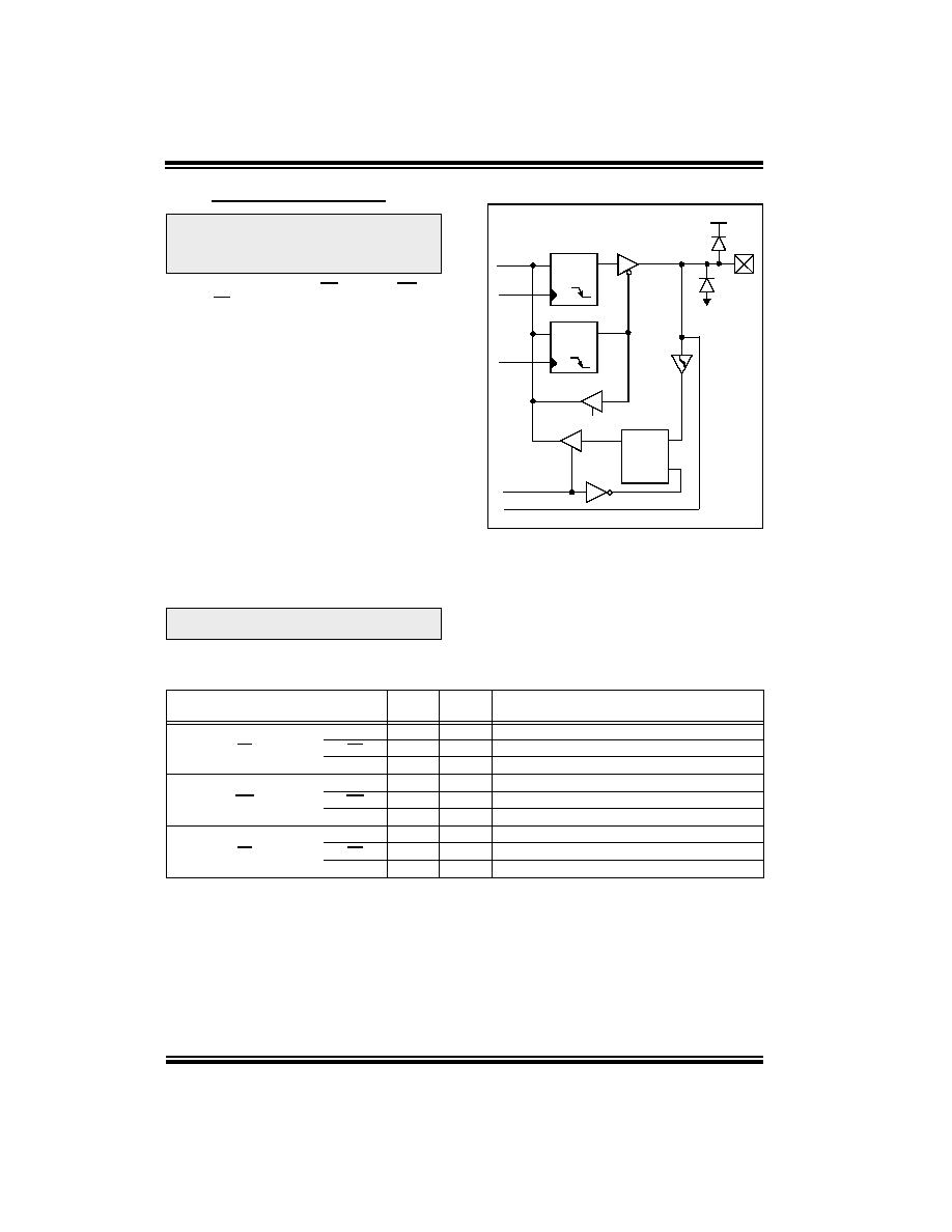
5.5
PORTE and TRISE Registers
PORTE has three pins, RE0/RD/AN5, RE1/WR/AN6
and RE2/CS/AN7, which are individually configured as
inputs or outputs. These pins have Schmitt Trigger
input buffers.
I/O PORTE becomes control inputs for the micropro-
cessor port when bit PSPMODE (TRISE<4>) is set. In
this mode, the user must make sure that the
TRISE<2:0> bits are set (pins are configured as digital
inputs) and that register ADCON1 is configured for dig-
ital I/O. In this mode, the input buffers are TTL.
Register 5-1 shows the TRISE register, which also con-
trols the parallel slave port operation.
PORTE pins may be multiplexed with analog inputs
(PIC16C765 only). The operation of these pins is
selected by control bits in the ADCON1 register. When
selected as an analog input, these pins will read as ’0’s.
TRISE controls the direction of the RE pins, even when
they are being used as analog inputs. The user must
make sure to keep the pins configured as inputs when
using them as analog inputs.
TRISE bits are used to control the parallel slave port.
FIGURE 5-7:
PORTE BLOCK DIAGRAM
TABLE 5-9:
PORTE(1) FUNCTIONS
Note 1: The
PIC16C745
does
not
provide
PORTE. The PORTE and TRISE registers
are reserved. Always maintain these bits
clear.
Note:
On a Power-on Reset, these pins are con-
figured as analog inputs.
Data
Bus
WR
Port
WR
TRIS
RD Port
Data Latch
TRIS Latch
RD TRIS
Schmitt
Trigger
Input
Buffer
Q
D
CK
Q
D
CK
EN
QD
EN
I/O pin
To A/D Converter
VDD
Name
Function
Input
Type
Output
Type
Description
RE0/RD/AN5
RE0
ST
CMOS
Bi-directional I/O(1)
RD
TTL
—
Parallel Slave Port Control Input(1)
AN5
AN
—
A/D Input(1)
RE1/WR/AN6
RE1
ST
CMOS
Bi-directional I/O(1)
WR
TTL
—
Parallel Slave Port Control Input(1)
AN6
AN
—
A/D Input(1)
RE2/CS/AN7
RE2
ST
CMOS
Bi-directional I/O(1)
CS
TTL
—
Parallel Slave Port Data Input(1)
AN7
AN
—
A/D Input(1)
Legend:
OD = open drain, ST = Schmitt Trigger
Note 1:
PIC16C765 only.
745cov.book Page 38 Wednesday, August 2, 2000 8:24 AM
发布紧急采购,3分钟左右您将得到回复。
相关PDF资料
PIC18C442T-E/L
IC MCU OTP 8KX16 A/D 44PLCC
PIC16C621A-40/SS
IC MCU OTP 1KX14 COMP 20SSOP
PIC16C622A-40/SS
IC MCU OTP 2KX14 COMP 20SSOP
PIC16CE623-30/SO
IC MCU OTP 512X14 EE COMP 18SOIC
PIC16CE624-30/SO
IC MCU OTP 1KX14 EE COMP 18SOIC
PIC16CE624-30/SS
IC MCU OTP 1KX14 EE COMP 20SSOP
PIC16CE623-30/SS
IC MCU OTP 512X14 EE COMP 20SSOP
PIC16CE624-30/P
IC MCU OTP 1KX14 EE COMP 18DIP
相关代理商/技术参数
PIC16C765T-I/PT
功能描述:8位微控制器 -MCU 14KB 256 RAM 33 I/O RoHS:否 制造商:Silicon Labs 核心:8051 处理器系列:C8051F39x 数据总线宽度:8 bit 最大时钟频率:50 MHz 程序存储器大小:16 KB 数据 RAM 大小:1 KB 片上 ADC:Yes 工作电源电压:1.8 V to 3.6 V 工作温度范围:- 40 C to + 105 C 封装 / 箱体:QFN-20 安装风格:SMD/SMT
PIC16C76T-04/SO
功能描述:8位微控制器 -MCU 14KB 368 RAM 22 I/O RoHS:否 制造商:Silicon Labs 核心:8051 处理器系列:C8051F39x 数据总线宽度:8 bit 最大时钟频率:50 MHz 程序存储器大小:16 KB 数据 RAM 大小:1 KB 片上 ADC:Yes 工作电源电压:1.8 V to 3.6 V 工作温度范围:- 40 C to + 105 C 封装 / 箱体:QFN-20 安装风格:SMD/SMT
PIC16C76T-04E/SO
功能描述:8位微控制器 -MCU 14KB 368 RAM 22 I/O RoHS:否 制造商:Silicon Labs 核心:8051 处理器系列:C8051F39x 数据总线宽度:8 bit 最大时钟频率:50 MHz 程序存储器大小:16 KB 数据 RAM 大小:1 KB 片上 ADC:Yes 工作电源电压:1.8 V to 3.6 V 工作温度范围:- 40 C to + 105 C 封装 / 箱体:QFN-20 安装风格:SMD/SMT
PIC16C76T-04I/SO
功能描述:8位微控制器 -MCU 14KB 368 RAM 22 I/O RoHS:否 制造商:Silicon Labs 核心:8051 处理器系列:C8051F39x 数据总线宽度:8 bit 最大时钟频率:50 MHz 程序存储器大小:16 KB 数据 RAM 大小:1 KB 片上 ADC:Yes 工作电源电压:1.8 V to 3.6 V 工作温度范围:- 40 C to + 105 C 封装 / 箱体:QFN-20 安装风格:SMD/SMT
PIC16C76T-10/SO
功能描述:8位微控制器 -MCU 14KB 368 RAM 22 I/O RoHS:否 制造商:Silicon Labs 核心:8051 处理器系列:C8051F39x 数据总线宽度:8 bit 最大时钟频率:50 MHz 程序存储器大小:16 KB 数据 RAM 大小:1 KB 片上 ADC:Yes 工作电源电压:1.8 V to 3.6 V 工作温度范围:- 40 C to + 105 C 封装 / 箱体:QFN-20 安装风格:SMD/SMT
PIC16C76T-10E/SO
功能描述:8位微控制器 -MCU 14KB 368 RAM 22 I/O RoHS:否 制造商:Silicon Labs 核心:8051 处理器系列:C8051F39x 数据总线宽度:8 bit 最大时钟频率:50 MHz 程序存储器大小:16 KB 数据 RAM 大小:1 KB 片上 ADC:Yes 工作电源电压:1.8 V to 3.6 V 工作温度范围:- 40 C to + 105 C 封装 / 箱体:QFN-20 安装风格:SMD/SMT
PIC16C76T-10I/SO
功能描述:8位微控制器 -MCU 14KB 368 RAM 22 I/O RoHS:否 制造商:Silicon Labs 核心:8051 处理器系列:C8051F39x 数据总线宽度:8 bit 最大时钟频率:50 MHz 程序存储器大小:16 KB 数据 RAM 大小:1 KB 片上 ADC:Yes 工作电源电压:1.8 V to 3.6 V 工作温度范围:- 40 C to + 105 C 封装 / 箱体:QFN-20 安装风格:SMD/SMT
PIC16C76T-20/SO
功能描述:8位微控制器 -MCU 14KB 368 RAM 22 I/O RoHS:否 制造商:Silicon Labs 核心:8051 处理器系列:C8051F39x 数据总线宽度:8 bit 最大时钟频率:50 MHz 程序存储器大小:16 KB 数据 RAM 大小:1 KB 片上 ADC:Yes 工作电源电压:1.8 V to 3.6 V 工作温度范围:- 40 C to + 105 C 封装 / 箱体:QFN-20 安装风格:SMD/SMT